- 您现在的位置:买卖IC网 > Sheet目录1996 > HMC700LP4E (Hittite Microwave Corporation)IC FRACT-N PLL 16BIT 24QFN
For price, delivery and to place orders: Hittite Microwave Corporation, 2 Elizabeth Drive, Chelmsford, MA 01824
978-250-3343 tel 978-250-3373 fax Order On-line at www.hittite.com
Application Support: apps@hittite.com
P
LL
-
F
r
a
c
t
io
n
a
L-
n
-
S
M
t
0
0 - 17
HMC700LP4 / 700LP4E
v11.0411
8 GHz 16-Bit Fractional-N PLL
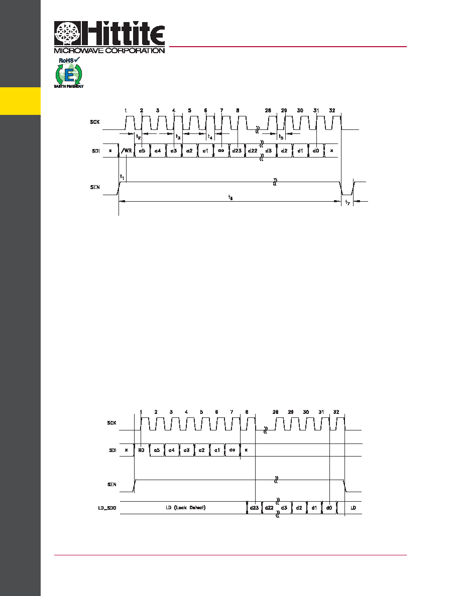
Figure 15. Serial Port Timing Diagram - Write Serial Port WRITE Operation
Serial Port READ Operation
a typical rEaD cycle is shown in Figure 16.
a. the Master (host) asserts both SEn (Serial Port Enable) and SDi to indicate a rEaD cycle, followed
by a rising edge ScK. note: the Lock Detect function is multiplexed onto the LD_SDo pin. it is
suggested that lock detect (LD) only be considered valid when SEn is low. in fact LD will not toggle
until the first active data bit toggles on LD_SDo, and will be restored immediately after the trailing
edge of the LSB of serial data out as shown in Figure 15.
b. the slave (synthesizer) reads SDi on the 1st rising edge of ScK after SEn. SDi high initiates the
rEaD cycle (rD).
c. Host places the six address bits on the next six falling edges of ScK, MSB first.
d. Slave registers the address bits on the next six rising edges of ScK (2-7).
e. Slave switches from Lock Detect and places the requested 24 data bits on SD_LDo on the next 24
rising edges of ScK (8-31), MSB first .
f. Host registers the data bits on the next 24 falling edges of ScK (8-31).
g. Slave restores Lock Detect on the 32nd rising edge of ScK.
h. SEn is de-asserted on the 32nd falling edge of ScK.
i. the 32nd falling edge of ScK completes the rEaD cycle.
Figure 16. Serial Port Timing Diagram - READ Serial Port Operation
发布紧急采购,3分钟左右您将得到回复。
相关PDF资料
HMC703LP4E
IC FRACT-N PLL W/SWEEPR 24QFN
HMC704LP4E
IC FRACT-N PLL 16BIT 24QFN
HMC830LP6GE
IC FRACT-N PLL W/VCO 40QFN
HMP8117CNZ
IC VIDEO DECODER NTSC/PAL 80PQFP
HMP8156ACNZ
IC VIDEO ENCODER NTSC/PAL 64MQFP
HSP45102SC-40Z
IC OSC NCO 40MHZ 28-SOIC
HSP45106JC-33Z
IC OSC NCO 33MHZ 84-PLCC
HSP45116AVC-52Z
IC OSC NCO 52MHZ 160-MQFP
相关代理商/技术参数
HMC700LP4ETR
制造商:Hittite Microwave Corp 功能描述:IC FRACT-N PLL 16BIT 24QFN 制造商:Hittite Microwave Corp 功能描述:HMC700 Series 8 GHz 16-Bit Prescaler Fractional-N PLL - 4x4 mm QFN-24
HMC701LP6C
制造商:HITTITE 制造商全称:Hittite Microwave Corporation 功能描述:8 GHz 16-BIT FRACTIONAL-N SYNTHESIZER
HMC701LP6C_10
制造商:HITTITE 制造商全称:Hittite Microwave Corporation 功能描述:8 GHz 16-BIT FRACTIONAL-N SYNTHESIZER
HMC701LP6CE
制造商:Hittite Microwave Corp 功能描述:IC SYNTHESIZER W/SWEEPER 40-QFN
HMC702LP6CE
制造商:Hittite Microwave Corp 功能描述:IC SYNTHESIZER W/SWEEPER 40-QFN
HMC702LP6CE_10
制造商:HITTITE 制造商全称:Hittite Microwave Corporation 功能描述:14 GHz 16-BIT FRACTIONAL-N SYNTHESIZER
HMC702LP6CE_11
制造商:HITTITE 制造商全称:Hittite Microwave Corporation 功能描述:14 GHz 16-BIT FRACTIONAL-N PLL
HMC703LP4E
功能描述:IC FRACT-N PLL W/SWEEPR 24QFN RoHS:是 类别:集成电路 (IC) >> 时钟/计时 - 时钟发生器,PLL,频率合成器 系列:- 标准包装:2,000 系列:- 类型:PLL 频率合成器 PLL:是 输入:晶体 输出:时钟 电路数:1 比率 - 输入:输出:1:1 差分 - 输入:输出:无/无 频率 - 最大:1GHz 除法器/乘法器:是/无 电源电压:4.5 V ~ 5.5 V 工作温度:-20°C ~ 85°C 安装类型:表面贴装 封装/外壳:16-LSSOP(0.175",4.40mm 宽) 供应商设备封装:16-SSOP 包装:带卷 (TR) 其它名称:NJW1504V-TE1-NDNJW1504V-TE1TR